There are several ways to convert current into voltage (called I/V or I/U conversion stage) and all of them are full of compromises. Please refer to our frequently asked questions (FAQ) section (by clicking here). Popular way to passively convert current into voltage is to use a resistor. Passive resistive approach (using a resistor of high value) unfortunately kills signal integrity and its dynamics (also contributes to an impedance mismatch), unless a very low value resistor (below 10 Ohms) and I/V interface transformer is employed. Nevertheless, using a high value resistor (larger than 20 Ohms) as I/V conversion method across current out of a DAC and a tube grid results in most cases in impedance mismatch. If the output and input impedances are not matched, the mismatch acts like a filter in the audible frequency spectrum, where in most cases low frequencies are lost. On top of that, the consecutive stages in the audio amplification chain loose the drive and the dynamics irreversibly. The earlier the impedance mismatch in the chain, the worse it is. The most detrimental impedance mismatch in digital sources known to me is between the digital transport and the SPDIF receiver of a DAC but that is a different topic for now.
A very small value resistor and many DACs in parallel minimize the impedance mismatch to some extent. However, the impedance mismatch occurs because all current out DACs are high output impedance devices and low input impedance is ideal for accurately converting currents. Unfortunately, all tubes are high input impedance devices by their nature and are not ideal partner to current out DACs. Unlike tubes, transistors are low input impedance devices. Therefore, ideal matching partner to a current out R2R DAC would be a transistor. Unfortunately, it is a very uncommon approach for a number of reasons. Despite large choice of transistors available, it is very hard to find a relatively good sounding transistor now days, which is also stable and linear in its behavior. On top of that since transistors are active device, their sound heavily depends on the quality of power supplies, which is also a very critical and under-delivered aspect in the industry. Most engineers now days do not even bother using R2R DACs with current output amongst other reasons because all modern Delta Sigma designs dogma and those Delta Sigma DACs have naturally an op-amp (which are plagued by their complexity and and the amount of negative feedback loops is used) built in their chip. However, all original R2R DAC came with only with current out. Given that, there has been a fashion to reject active I/V conversion for numerous reasons. One of them is the notion that active devices are less perfect (speak linear) than passive. The other reason of rejecting active I/V is because of the cutting corners, one design fits all approach practiced by the majority in the industry. One would simply rely on using op-amps (containing around 30-40 transistors and resistors with plenty of negative feedback loops) even with Delta Sigma type of chips, therefore inevitably falling into the over-engineering trap.
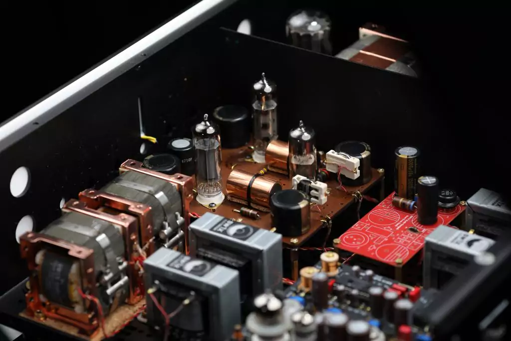
After some in depth experimentation, we came to a conclusion that a single transistor approach is the least compromised way (apart from utilizing a transformer) of converting current to voltage accurately, with an optimum signal transfer behavior. It preserves signal integrity and enhances dynamics unlike the passive resistor based approach. We feel that the potential of most current output R2R DACs (e.g. NOS TDA1543) is far from being fulfilled with an interpretation based on passive resistor I/V conversion with or without triode tube output stage. Instead we opted for a single vintage transistor per channel of highest possible material quality (which contains gold and palladium) powered by a shunt Germanium transistor voltage regulated based power supply. Everything else being equal, the difference in dynamics and low level musical information between passive resistor I/V and the active transistor I/V is like a comparison of 6 cylinder simple petrol engine (passive resistor) and a supercharged (active transistor) 12 cylinder diesel engine. Our active I/V approach transforms the TDA1543 (or any current out R2R DAC chip) into a different level of a DAC.
The issue of impedance mismatch is critical in 2 places of a DAC design: A) Between the current out of DAC chip after the I/V conversion and B) Between the first amplification output stage and the preamp/power amp input. Most common approach in the current out (best possible quality output of an R2R chip, which is impossible with Delta Sigma chips) DAC implementation is to use a passive shunt resistor as I/V converter. This approach works fine but has some drawbacks: the shunt resistor worsens the impedance mismatch further and it takes energy away, therefore some of the dynamics are irreversibly lost and all subsequent stage are lacking the drive. We, at SW1X Audio Design™ on the other hand, addressing the point A) by using a single transistor that does the job of I/V conversion, lowers the output impedance after the I/V stage (the DAC chip sees only 10 Ohm input impedance) and preserves the dynamics. Plus this approach allows us to use a simple but elegant class A, zero feedback valve output stage with low output impedance, which addresses impedance mismatch issue in the point B). On top of that the circuit remains elegant and simple and makes the music come alive with incredible dynamics and extreme analogue smoothness.
The only other way that insures signal integrity and an excellent signal transfer behavior is to employ a low value resistor in combination with an interface transformer. An I/V interface transformer, has been misleadingly labeled as a I/V conversion method. In fact, it does not perform any I/V conversion. A transformer with 1:1 ratio does neither transforms any current or voltage nor does it any conversion per se. The I/V conversion is actually performed by a lower value resistor after or before the transformers. The actual function of the I/V interface transformers is twofold: filtering ultrasonic noise and lowerering the input impedance therefore minimizing the impedance mismatch (since all tubes have very high input impedance) and maximizing the energy transfer i.e. preserving dynamics. Unless the interface transformer and the I/V resistor are of highest quality, one could call the interface transformer/resistor approach of least compromises. However, neither are transformers perfect devices and the cost of making transformers with the quality required can be immense and are unsuitable for lower priced products.
Slawa Roschkow, 10. 2015
 Conversion)