The most overlooked issue that we are addressing in our designs is the impedance mismatch across various stages. If the output and input impedances are not matched, the mismatch acts like a filter in the audible frequency spectrum, where in most cases low frequencies are lost. On top of that, the consecutive stages in the audio amplification chain loose the drive and the dynamics irreversibly. The earlier the impedance mismatch in the chain, the worse it is. The most detrimental impedance mismatch in digital sources known to me is between the digital transport and the S/PDIF receiver of a DAC but that is a different topic for now.
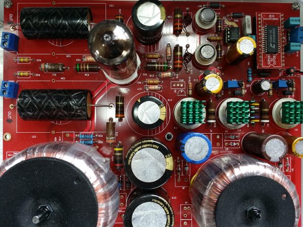
The issue of impedance mismatch is critical in 2 places of a DAC design: A) Between the current out of DAC chip after the I/V conversion and B) Between the first amplification output stage and the preamp/power amp input. Most common approach in the TDA1543 DAC implementation is to use a passive shunt resistor as I/V converter. This approach works fine but has some drawbacks: the shunt resistor worsens the impedance mismatch further and it takes energy away, therefore some of the dynamics are irreversibly lost and all subsequent stage are lacking the drive.
In order to avoid the mismatch in impedances, the output impedance needs to be ideally be multiples time lower than the input impedance. However, the current out DAC chips such as TDA1543 has high impedance output by nature but likes to see a low impedance input of the next stage. That is not happening if the next input stage is a valve since valves have high impedance input by nature. In order to minimise the mismatch, many designs are using multiple TDA1543 DAC chips in parallel in order to lower the output impedance before the I/V stage. The drawback here is that voltage output after the conversion becomes relatively high, actually already high enough to saturate some of the preamp inputs. Therefore most DAC designs stop here and have no output stage. However, that solution causes the problem of impedance mismatch in point B) especially when valves and passive preamps are used in between.
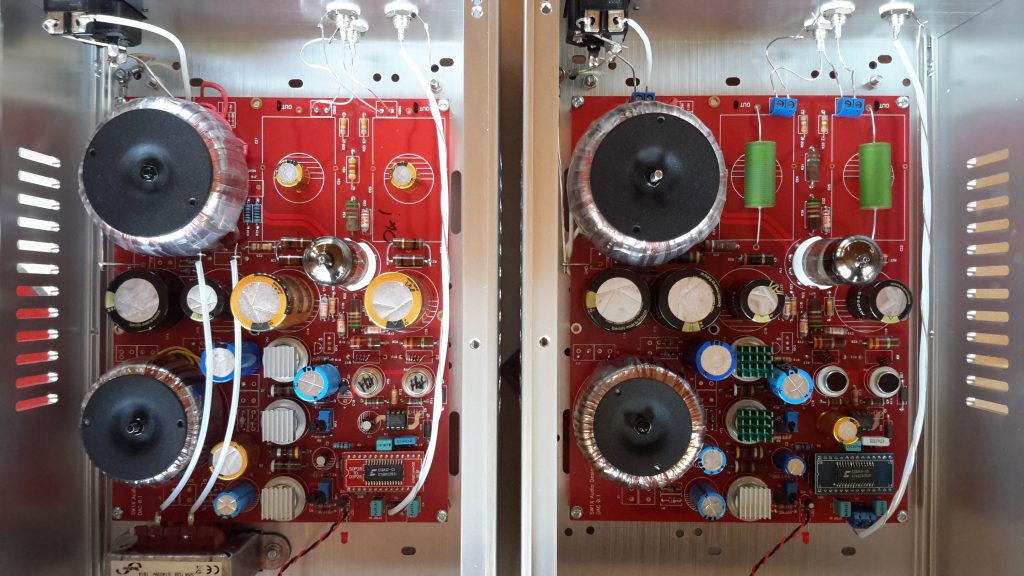
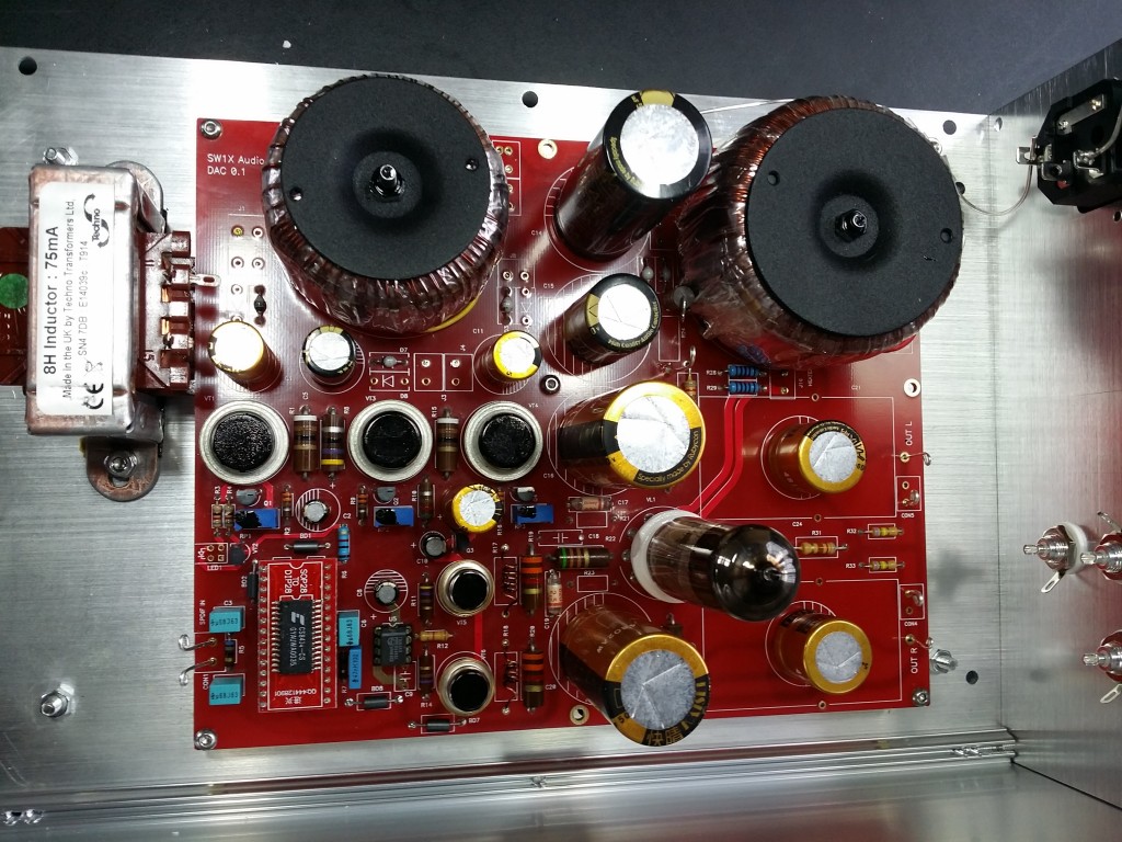
We at SW1X Audio Design™, on the other hand addressing the point A) by using a single transistor that does the job of I/V conversion, which provides low input impedance to current out of a DAC, lowers output impedance after the I/V stage and therefore preserves the signal integrity and the dynamic envelope of music. Plus this approach allows us to use a simple but elegant class A, zero feedback valve output stage with low output impedance, which addresses impedance mismatch issue in the point B). On top of that the circuit remains elegant and simple and makes the music come alive with incredible analogue smoothness.
The other important application is power supplies. Power supplies matter a lot because they are directly influencing the quality of sound. Here we have opted out for shunt voltage regulated power supplies based on elegantly simple implementation of a vintage Germanium transistor. The difference in sound over a off-the shelf industrial IC based voltage regulator such as LM317 is immense. Everything else being equal, all industrial grade IC voltage regulators we came across are characterised by grayish graininess, lack of colour and dynamics sound. Our own custom designed shunt voltage regulator does exactly the opposite by bringing clarity, transparency, vivid colours, juice and dynamics back into the sound.
Slawa Roschkow, 11.11.2015